What is the MOSFET Threshold Voltage?
The threshold voltage (Vth) of a MOSFET is the gate-to-source voltage at which a conducting channel begins to form between the source and drain. Below this voltage the transistor is essentially off; above it, the device turns on. Vth is one of the most important parameters in transistor and analog/digital circuit design, setting bias points, logic levels, and leakage behavior.
The Formula
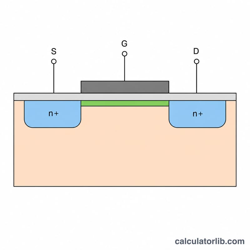
For an n-channel (NMOS) device built on a p-type substrate, the long-channel threshold voltage is:
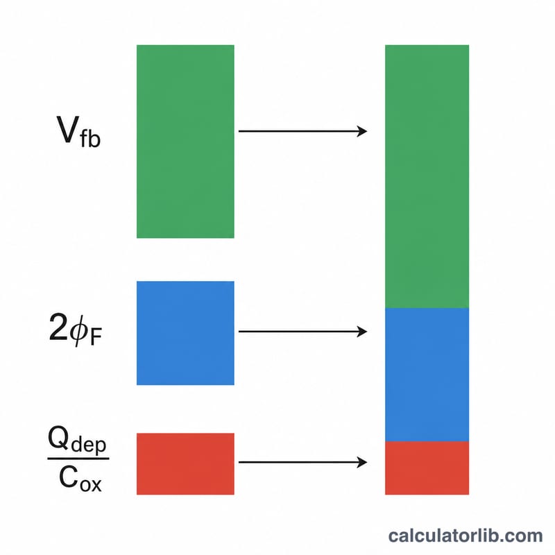
$$V_{th} = V_{fb} + 2\phi_F + \frac{\sqrt{2\,\varepsilon_s\, q\, N_a \cdot 2\phi_F}}{C_{ox}}$$
where \(V_{fb}\) is the flat-band voltage, \(\phi_F\) is the Fermi potential, \(\varepsilon_s = \varepsilon_r \cdot \varepsilon_0\) is the silicon permittivity (\(\varepsilon_0 \approx 8.854\times10^{-14}\) F/cm), \(q = 1.602\times10^{-19}\) C is the electron charge, \(N_a\) is the substrate acceptor doping concentration (cm⁻³), and \(C_{ox}\) is the gate-oxide capacitance per unit area (F/cm²). The \(2\phi_F\) term sets the strong-inversion surface potential, and the square-root term is the voltage needed to support the depletion-region (body) charge.
How to Use It
Enter the flat-band voltage, Fermi potential, substrate doping, oxide capacitance, and the relative permittivity of silicon (default 11.7). Keep all quantities in CGS-compatible units: doping in cm⁻³ and capacitance/permittivity per cm². The calculator returns \(V_{th}\) along with the surface-inversion term and the depletion-charge term so you can see how each contributes.
Worked Example
Take \(V_{fb} = -0.9\) V, \(\phi_F = 0.3\) V, \(N_a = 1\times10^{16}\) cm⁻³, \(C_{ox} = 3.45\times10^{-7}\) F/cm², \(\varepsilon_r = 11.7\). Then \(\varepsilon_s = 1.036\times10^{-12}\) F/cm. The inside of the root is $$2 \cdot \varepsilon_s \cdot q \cdot N_a \cdot 0.6 = 1.992\times10^{-15},$$ whose square root is \(\approx 4.463\times10^{-8}\) C/cm². Dividing by \(C_{ox}\) gives \(\approx 0.1294\) V. So $$V_{th} = -0.9 + 0.6 + 0.1294 \approx -0.171 \text{ V}.$$
FAQ
Does this work for PMOS? The same structure applies, but signs of \(V_{fb}\), \(\phi_F\), and doping type flip; this tool models the NMOS case.
What units should I use? Use cm-based units (cm⁻³ for doping, F/cm² for capacitance) so that the embedded constants \(q\) and \(\varepsilon_0\) are consistent.
Why is Vth sometimes negative? A negative \(V_{th}\) (depletion-mode device) can result when the flat-band voltage is strongly negative relative to the inversion and body terms.